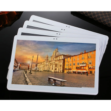
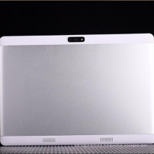
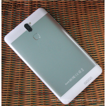

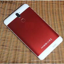
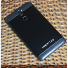

ENIG and OSP mobile HDI circuit boards
Basic Info
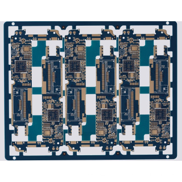
Model No.: CW-310
Product Description
Continued growth in handset production drives demand for HDI board growth China plays an important role in the world's mobile phone manufacturing industry. Since Motorola made full use of HDI boards to manufacture mobile phones in 2002, more than 90% of mobile phone motherboards now use HDI boards.
Electronic design is also trying to reduce its size while continuously improving the performance of the whole machine. From mobile phones to smart small portable products, small is always the same pursuit. High-density integration (HDI) technology enables end-product design to be more compact while meeting higher standards of electronic performance and efficiency. HDI is currently widely used in mobile phones, digital (camera) cameras, MP3, MP4, notebook computers, automotive electronics and other digital products, among which mobile phones are the most widely used. HDI boards are generally manufactured using a build-up method. The more times the layers are stacked, the higher the technical grade of the board. Ordinary HDI boards are basically one-time laminate, high-order HDI uses two or more layers of technology, and adopts advanced PCB technology such as stacking holes, plating holes, and laser direct drilling. High-end HDI boards are mainly used in 3G mobile phones, advanced digital video cameras, IC carrier boards, etc.

Specifications:
Material: FR4, S1000
Layer: 8L
Copper thickness: 1OZ
Board thickness: 1.2mm
Surface Finishing: Immersion gold + OSP
Solder mask color: Blue
Silkscreen color: White
Describe: HDI 1+N+1, Blind and buried holes, 3/3 mil

________________________________________________________________________________________________________________________________________________________
Printed circuit boards abbreviation as PCB. A conductive pattern which is formed on a dielectric material in a predetermined design to form a printed circuit, a printed component, or a combination of the two is generally referred to as a printed circuit. And a conductive pattern that provides electrical connection between components on an insulating substrate, called printed circuits.
PCB characteristics
● High density. For decades, the high density of printed boards has grown with the increased integration of integrated circuits and advances in mounting technology.
● High reliability. Through a series of inspections, tests and aging tests, the PCB can be reliably operated for a long period of time (usually 20 years).
● Designability. For the various performances of PCB (electrical, physical, chemical, mechanical, etc.), the design of printed boards can be realized through design standardization and standardization, with short time and high efficiency.
● Productivity. With modern management, it can carry out standardization, scale (quantity), automation and other production to ensure product quality consistency.
● Testability. Established relatively complete test methods, test standards, various test equipment and instruments to detect and identify PCB product qualification and service life.
● Assemblyability. PCB products not only facilitate the standardized assembly of various components, but also can be automated, large-scale mass production. At the same time, the PCB and various component assembly components can be assembled to form larger components and systems up to the complete machine.
● Maintainability. Since PCB products and various component assembly components are produced in a standardized design and scale, these components are also standardized. Therefore, once the system fails, it can be replaced quickly, conveniently and flexibly, and the system can be quickly restored. Of course, you can say more about it. Such as miniaturization and weight reduction of the system, high-speed signal transmission, etc.
__________________________________________________________________________________________________________________________________________
ChuangYing Electronics
FOUR Advantages Quality with promise
More than 15 years Team Pursuit of first-class quality
1, About the factory--More than 15 years industry experience: Self-built factory, 15 years of focus on circuit board manufacturing.
☆ Flip Aluminium PCB: The share of Aluminum industry more than 45%, service and quality have won the praise of customers.
☆ Advanced equipment: PVC plating line, CNC V-CUT machine, Dongtai high speed drilling machine, high speed flying probe testing machine, microscope, copper foil tensile tester, ion pollution degree detector.
2, Top technical team - fast delivery, professional service
☆ 50 professional and technical people with more than 10 years of PCB experience have rich experience in various industry standards and process quality requirements.
☆ Provide after-sales technical support, quickly respond to bad feedback, solve customer's difficult problems
3, Certifications - UL, IO9001:2015, ISO14001:2015, IATF16949
☆ All products undergo strict SGS testing and meet ROHS requirements
☆ Implement TQM quality management and 6σ management mode, continuous improvement, good rate 99%
☆ Quality control seniors are skilled in IATF16949, QS9000 requirements,and have their internal auditor qualification certificate
4.Work with well-known companies - trustworthy PCB manufacturers
☆ Over the years, has business contacts with many well-known companies such as BYD, Huawei, Schneider, and Siemens etc., and has maintained long-term supply relationships with these industry benchmarking companies.
☆ The products are exported to Europe, America, Japan, Middle East, Philippines and other overseas markets, and are well received and trusted by customers.
Contact us if you need more details on ENIG and OSP Two Finishing PCB. We are ready to answer your questions on packaging, logistics, certification or any other aspects about Mobile HDI Printed Circuit Boards、0.1mm Holes 0.075mm Lines HDI Board. If these products fail to match your need, please contact us and we would like to provide relevant information.Product Categories : HDI PCB > Blind And Buried Hole PCB